Shining a Light on EUV Lithography: The Future of Semiconductor Manufacturing

Introduction to Extreme Ultraviolet Lithography (EUV)
Extreme Ultraviolet (EUV) lithography is a cutting-edge technology revolutionizing the semiconductor fabrication industry. This advanced process uses extremely short wavelength light (13.5 nm) to print intricate patterns onto silicon wafers, producing smaller, faster, and more power-efficient microchips. EUV lithography has become a critical tool in developing next-generation electronics, from smartphones and laptops to artificial intelligence and 5G networks.
As the demand for more powerful and compact devices continues to grow, EUV technology has emerged as a key enabler for the semiconductor industry to keep pace with Moore's Law, which predicts the doubling of transistors on a chip every two years. EUV lithography has opened up new possibilities for innovation and performance in the digital age by allowing chipmakers to pack more transistors onto a single chip.
In this blog post, we will delve into the world of EUV lithography, its technical intricacies, the competitive landscape of EUV machine manufacturers, and the prospects of this transformative technology. We will examine the challenges and breakthroughs in developing EUV systems, the geopolitical implications of this strategic technology, and its widespread adoption's environmental and economic impact. By the end of this post, you will have a comprehensive understanding of EUV lithography and its pivotal role in shaping the future of computing and electronics.
The Mechanics of EUV Machines
At the heart of EUV lithography lies a complex system of advanced optics, powerful lasers, and precise control mechanisms. Unlike traditional photolithography, which uses visible or ultraviolet light to transfer patterns onto silicon wafers, EUV lithography employs extreme ultraviolet light with a wavelength of just 13.5 nanometers. This incredibly short wavelength creates much smaller and more intricate patterns, enabling the production of cutting-edge microchips with billions of transistors.

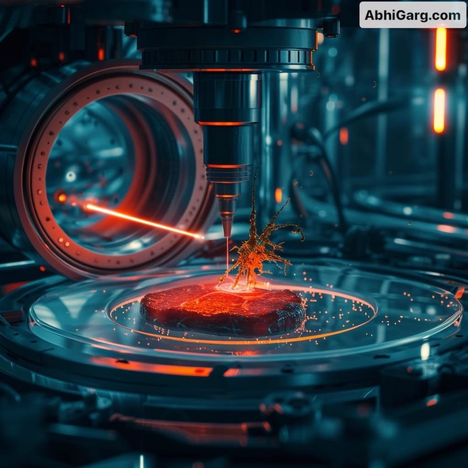
The process begins with the generation of EUV light, which is produced by firing a high-powered laser at microscopic droplets of molten tin. The intense heat from the laser causes the tin to emit EUV photons, which are then collected and focused by a series of mirrors coated with highly reflective multilayer materials. These mirrors guide the EUV light through a complex optical system, which includes a mask with the desired chip pattern and a series of lenses that reduce and focus the image onto the silicon wafer.
One of the main challenges in developing EUV lithography has been creating suitable optics. Because EUV light is absorbed by nearly all materials, traditional lenses and mirrors cannot be used. Instead, EUV systems rely on a series of specially designed multilayer mirrors that reflect the light at a specific angle. These mirrors must be manufactured to exceptional levels of precision, with surface smoothness measured in picometers (trillionths of a meter).
Another critical component of EUV machines is the vacuum environment in which the lithography process occurs. Because EUV light is easily absorbed by air, the entire system must operate in a near-perfect vacuum to ensure the light reaches the wafer with minimal loss. This requires sophisticated pumping systems and ultra-clean manufacturing environments to prevent contamination.
Despite these challenges, the development of EUV lithography has been driven by the relentless demand for faster, smaller, and more efficient microchips. With each new generation of EUV machines, manufacturers have been able to push the boundaries of what is possible, creating chips with features measuring just a few nanometers wide. As technology continues to evolve, it is expected to play a crucial role in enabling the next wave of digital innovation, from artificial intelligence and 5G networks to the Internet of Things and beyond.
The Market Landscape of EUV Lithography
A handful of key players dominate the EUV lithography machine market, each vying for a share of this lucrative and strategically important industry. Dutch manufacturer ASML Holding N.V. has emerged as the clear leader, with a market share of over 80% in EUV lithography systems. ASML's success can be attributed to its early investment in EUV technology and its close partnerships with leading chipmakers such as Intel, Samsung, and TSMC.
ASML's primary competitor is Nikon Corporation, a Japanese company with a long history in lithography systems. While Nikon has been slower in embracing EUV technology, it has recently made significant investments in this area, aiming to challenge ASML's dominance. Other players in the market include Canon Inc., another Japanese manufacturer, and China-based Shanghai Micro Electronics Equipment (SMEE), which has been working to develop its own EUV systems as part of China's push for semiconductor self-sufficiency.
High barriers to entry characterize the EUV lithography market. The development of these complex machines requires significant capital investment and technical expertise. As a result, the market is expected to remain consolidated in the near future, with ASML and Nikon likely to maintain their leadership positions.
However, the growing demand for EUV lithography systems, driven by the increasing complexity of microchips and the proliferation of connected devices, is attracting new entrants to the market. In particular, the rise of Chinese manufacturers, backed by government support and domestic demand, could reshape the competitive landscape in the coming years.
The EUV lithography market is also being shaped by broader trends in the semiconductor industry, such as the shift towards fabless manufacturing and the increasing importance of advanced packaging techniques. As chipmakers look to outsource more of their production to specialized foundries, the demand for EUV lithography systems is expected to grow, driving innovation and investment in this critical technology.
Overall, the EUV lithography machine market is poised for significant growth in the coming years, with analysts projecting the market to reach over $20 billion by 2025. As the race to develop smaller, faster, and more efficient microchips continues, EUV technology is set to play a pivotal role in enabling the next generation of electronic devices and applications.
Geopolitical Implications in the EUV Sector
The development and control of EUV lithography technology have significant geopolitical implications, with governments worldwide recognizing the strategic importance of this critical enabler of advanced microchips. The United States, Japan, South Korea, and the Netherlands have all identified EUV lithography as a key national security priority, investing heavily in research and development and implementing policies to protect their domestic industries.

In particular, the ongoing trade tensions between the United States and China have brought the EUV lithography sector into sharp focus. The U.S. government has imposed strict export controls on EUV technology, citing concerns over China's use of advanced microchips for military and surveillance purposes. These controls have prevented Chinese companies from accessing the latest EUV lithography systems, hindering their ability to produce cutting-edge semiconductors.
In response, China has redoubled its efforts to develop its own EUV technology, investing billions of dollars in domestic research and development and seeking to acquire foreign expertise through talent recruitment and industrial espionage. This has raised concerns among Western governments and companies, who fear that China's rise as a semiconductor powerhouse could undermine their competitive positions and national security interests.
The competition over EUV technology has also led to political one-upmanship, with countries using their control over key components and materials as leverage in trade negotiations. For example, in 2019, the Japanese government restricted exports of high-purity hydrogen fluoride, a critical material used in EUV lithography, to South Korea, citing concerns over national security. This move was widely seen as retaliation for a South Korean court ruling on wartime labor compensation, highlighting the complex interplay between politics and technology in the EUV sector.
As the geopolitical stakes continue to rise, governments and companies increasingly focus on securing access to EUV lithography technology and protecting their intellectual property. This has led to a growing emphasis on domestic production and supply chain resilience as countries seek to reduce their dependence on foreign suppliers and maintain their competitive edge in the global semiconductor industry.
Innovations and Technological Advancements in EUV Lithography
Constant innovations and technological advancements have driven the rapid evolution of EUV lithography technology as manufacturers seek to push the boundaries of what is possible in semiconductor fabrication. One of the most significant recent developments has been the emergence of high numerical aperture (high-NA) EUV systems, which promise further to extend the resolution and productivity of EUV lithography.
High-NA EUV systems use a larger aperture and a more complex set of mirrors to focus the EUV light onto the wafer, creating even smaller and more intricate patterns. This technology is expected to allow chipmakers to produce microchips with feature sizes of 3 nanometers or less, compared to the 7-nanometer chips currently in production using standard EUV lithography.
ASML has led the development of high-NA EUV systems. It has invested heavily in this technology and has already secured orders from major chipmakers such as Intel and TSMC. The company's first high-NA EUV system, the EXE:5000, is expected to produce 1.5 million wafers annually.
Another key area of innovation in EUV lithography has been the development of new materials and processes to improve the technology's efficiency and reliability. For example, researchers have been working on new types of photoresists, the light-sensitive materials used to transfer patterns onto the wafer, that can withstand the intense energy of EUV light without degrading or causing defects.
Similarly, manufacturers have been developing new methods for repairing and maintaining the delicate multilayer mirrors used in EUV systems. These mirrors can become damaged over time due to the high-energy photons and particles generated during lithography. These advances are critical for ensuring the long-term viability and cost-effectiveness of EUV lithography as a manufacturing technology.
The impact of these innovations on the semiconductor industry cannot be overstated. By enabling the production of smaller, faster, and more power-efficient microchips, EUV lithography is driving the development of a wide range of new technologies and applications, from 5G networks and artificial intelligence to autonomous vehicles and the Internet of Things.
For example, the increased transistor density enabled by EUV lithography allows chipmakers to create more powerful and efficient processors for smartphones and laptops, extending battery life and enabling new features such as high-resolution displays and advanced camera systems. Similarly, the ability to produce smaller and more specialized chips opens up new possibilities for edge computing and deploying AI algorithms in devices such as smart sensors and industrial machinery.
As the demand for these advanced technologies continues to grow, the importance of EUV lithography as a key enabler of innovation will only increase. With each new generation of EUV systems, manufacturers are pushing the boundaries of what is possible in semiconductor fabrication, driving the digital transformation of industries and societies worldwide.
The Future of EUV Technology and Its Challenges
As EUV lithography continues to advance, it is poised to play an increasingly critical role in the future of semiconductor manufacturing. However, the path forward has challenges as the industry grapples with the technical limitations, supply chain issues, and scaling difficulties associated with this complex technology.
One of the primary challenges facing EUV lithography is the need for continued improvements in resolution and throughput. While high-NA EUV systems promise to extend the technology's resolution beyond the 3-nanometer node, achieving this will require further optics, materials, and process control advancements. At the same time, manufacturers must find ways to increase the productivity of EUV systems, which currently need to catch up to traditional lithography methods in terms of wafers per hour.
Another key challenge for the EUV industry is the need to scale production to meet the growing demand for advanced microchips. This will require significant investments in new manufacturing facilities and equipment and the development of a robust supply chain for key components and materials. With EUV systems costing upwards of $150 million each, the capital requirements for scaling production are immense and require close collaboration between chipmakers, equipment manufacturers, and governments.
The semiconductor industry increasingly turns to research institutions and government support to address these challenges to drive innovation and investment in EUV technology. For example, the U.S. government has recently launched several initiatives to strengthen the domestic semiconductor supply chain, including the CHIPS for America Act, which provides funding for research and development in advanced lithography and other critical technologies.

Similarly, research institutions worldwide are working to develop new materials, processes, and design methodologies that can help overcome the technical limitations of EUV lithography. For example, researchers at the University of California, Berkeley, have developed a new type of photoresist that is more sensitive to EUV light, enabling the creation of even smaller and more intricate patterns on the wafer.
Despite these challenges, the future of EUV lithography looks bright, with the technology expected to remain a key driver of innovation in the semiconductor industry for years to come. As manufacturers continue to push the boundaries of what is possible with EUV, we can expect to see a new wave of advanced microchips that are smaller, faster, and more power-efficient than ever before.
This, in turn, will enable a wide range of new technologies and applications, from 5G networks and artificial intelligence to autonomous vehicles and the Internet of Things. As the world increasingly relies on these advanced technologies, the importance of EUV lithography as a critical enabler of innovation will only continue to grow.
The Environmental and Economic Impact of EUV Adoption
As EUV lithography becomes more widely adopted in the semiconductor industry, it is important to consider this technology's environmental and economic implications. On the environmental front, the use of EUV systems presents both challenges and opportunities. The production of EUV light requires significant amounts of energy, and using materials such as tin and hydrogen in the process can create waste and emissions that must be carefully managed.
At the same time, however, the increased efficiency and performance of EUV-manufactured microchips can help to reduce the overall energy consumption and environmental impact of electronic devices. By enabling the creation of smaller, more power-efficient chips, EUV technology can help to extend the battery life of smartphones and laptops, reduce the energy requirements of data centers and communication networks, and support the development of more sustainable technologies such as electric vehicles and renewable energy systems.
From an economic perspective, the adoption of EUV lithography is expected to impact the semiconductor industry and the broader technology sector significantly. The high cost and complexity of EUV systems are likely to drive further consolidation in the industry, as only the largest and most well-funded companies will be able to afford the investments required to maintain a competitive edge.
At the same time, however, the increased performance and functionality of EUV-manufactured chips are expected to create new market opportunities and drive innovation across a wide range of industries. As the demand for advanced microchips continues to grow, the economic impact of EUV technology is likely to be felt not only in the semiconductor industry but also in the broader technology sector and the global economy.
Balancing the environmental and economic implications of EUV adoption will require close collaboration between industry, government, and academic stakeholders. By working together to develop sustainable manufacturing practices, invest in research and development, and support the growth of a robust and resilient semiconductor supply chain, we can ensure that the benefits of this transformative technology are realized while minimizing its negative impacts.
Conclusion: EUV Lithography as a Catalyst for Change
EUV lithography represents a major milestone in the evolution of semiconductor manufacturing, potentially transforming how we design, produce, and use electronic devices. As this technology advances, it is poised to become a key enabler of innovation across various industries, from communications and computing to healthcare and transportation.
While the challenges associated with EUV lithography are significant, from the technical complexities of the technology to the geopolitical tensions surrounding its development and deployment, the potential benefits are too great to ignore. By pushing the boundaries of what is possible in semiconductor fabrication, EUV technology is opening up new frontiers in performance, efficiency, and functionality, paving the way for a new era of digital innovation.
FAQs
- What is the main advantage of EUV lithography over traditional lithography methods?
EUV lithography uses extremely short wavelength light (13.5 nm), enabling the production of smaller, faster, and more power-efficient microchips compared to traditional lithography methods. - Who are the major players in the EUV lithography machine market?
The main players in the EUV lithography machine market are ASML Holding N.V. (Netherlands), Nikon Corporation (Japan), Canon Inc. (Japan), and Shanghai Micro Electronics Equipment (China). - What are the key challenges in developing EUV lithography technology?
Some of the main challenges include creating suitable optics that can reflect EUV light, maintaining a near-perfect vacuum environment, and managing the high costs and complexity of EUV systems. - How does the geopolitical landscape impact the EUV lithography sector?
Governments recognize the strategic importance of EUV technology and have implemented policies, such as export controls and investment in domestic research, to protect their national interests and maintain competitive advantages. - What are high numerical aperture (high-NA) EUV systems, and how do they differ from standard EUV systems?
High-NA EUV systems use a larger aperture and more complex mirrors to focus EUV light onto the wafer, creating even smaller and more intricate patterns than standard EUV systems. - How does the adoption of EUV lithography impact the environment?
While EUV systems require significant energy and resources, the increased efficiency of EUV-manufactured microchips can help reduce electronic devices' overall environmental impact by extending battery life and reducing energy consumption. - What role do research institutions and governments play in advancing EUV lithography technology?
Research institutions and governments are critical in driving innovation and investment in EUV technology through initiatives such as funding for research and development, collaborations with industry partners, and developing a robust semiconductor supply chain.


